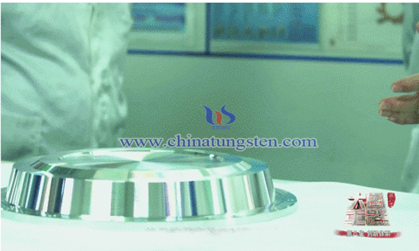
Tungsten Target Breaks Japan-US Monopoly
- Details
- Category: Tungsten's News
- Published on Wednesday, 13 February 2019 21:39
According to CCTV Finance and Economics Channel, in the past five years, China's contribution rate of scientific and technological progress to GDP has increased from 52.2% in 2012 to 57.5%, and the global ranking of national innovation ability has risen from 20th to 17th. Mechanisms, talents and finance, like fine-knitted nerve networks and blood vessels, constantly nourish China's steel and iron bones. This is another important tool for manufacturing National Heavy implements - China's unique system fertile soil, which is gathering the most lasting and deepest innovative force.

Blue whale No. 1, Sky Eye, Large Aircraft, Domestic Aircraft Carrier, a large country's heavy artillery brilliant appearance, so that the Chinese people are proud and the world admires. Behind these remarkable achievements, all of them reflect China's unique advantages in concentrating its efforts on major affairs. In the report, CCTV also mentioned a kind of heavy equipment used in the manufacture of large scale integrated circuits: ultra-pure metal sputtering target.
Ultra-high purity metal sputtering target is the necessary equipment for chip manufacturing. It is mainly used in 300 mm VLSI manufacturing. Its material purity requirement is more than 99.999%. This also involves the application of tungsten. In view of this, the editor solemnly introduces today's protagonist, tungsten target.
In the international mainstream large scale integrated circuit manufacturing, sputtering is one of the main technologies to prepare thin film materials. It emits atoms generated by high-speed moving ions bombarding target materials to accumulate on the surface of the substrate, forming a coating. The bombarded solid metal is the raw material of sputtering deposition film, called sputtering target material. Sputtering target is the necessary raw material for VLSI manufacturing. Before that, only a few multinational corporations in Japan and the United States could manufacture it. Therefore, our VLSI manufacturing has been blocked by invisible technical barriers in developed countries.
Rare metal tungsten is widely used in semiconductor integrated circuits, solar photovoltaic and other sputtering fields because of its high melting point, high strength, low thermal expansion coefficient, low resistivity and good thermal stability. Tungsten target is mainly used as diffusion barrier layer of integrated circuit and memory electrode of large scale integrated circuit in semiconductor field.
Semiconductor integrated circuits have high requirements for the purity of target materials. Generally, the purity of target materials is required to be more than 99.999%. At the same time, the compactness of the target material also has an important influence on the coating process and the performance of the film. The compactness of the target material not only affects the deposition rate, the density of the sputtered film particles and the discharge phenomenon, but also affects the electrical and optical properties of the sputtered film. The denser the target, the lower the density of the sputtered film particles, the weaker the discharge phenomenon, and the better the performance of the film. But correspondingly, tungsten has a high melting point. We use the traditional powder metallurgy method. Although the finished products can be fired, the quality and performance of tungsten are not stable, and it is difficult to burn large tungsten targets.
As the chip industry is the commanding point of high technology, an important strategic area, and the target material is the necessary equipment for chip manufacturing, and with the rapid development of semiconductor technology, the degree of integration is getting higher and higher. The number of integrated devices per unit area of single crystal silicon wafer is exponentially increasing. The mainstream size of silicon wafer has gradually developed from 12 inches (300 mm) to 18 inches (450 mm), so how to make it? Making larger size and high quality tungsten target has become a hot spot in tungsten product smelting.
At present, China has built the world's largest integrated circuit target manufacturing line, most of the supporting industries are basically perfect, and achieved the mass production of the whole series of products, providing more than 280 chip manufacturing plants worldwide. The content of impurities in ultra-pure metal sputtering targets is less than one-hundred-thousand; it is used in the manufacture of the world's leading 10-28 nanometer technology VLSI chips. In the harvest season, Huawei has been able to design and manufacture advanced smartphone chips independently by the Chinese people, and Ziguang can produce DR4 memory chips that break the world's oligopoly in science and technology. No country dares to despise China's position in the large-scale integrated circuit industry any more. (China Tungsten Online: Weiping)
- Tungsten Manufacturer & Supplier, Chinatungsten Online: www.chinatungsten.com
- Tungsten News & Prices of China Tungsten Industry Association: www.ctia.com.cn
- Molybdenum News & Price: news.molybdenum.com.cn
- Tel.: 86 592 5129696; Fax: 86 592 5129797; Email: sales@chinatungsten.com


 sales@chinatungsten.com