Rare Earth Prices - July 29, 2019
- Details
- Category: Tungsten's News
- Published on Monday, 29 July 2019 18:09
- Written by Shuxia
- Hits: 684
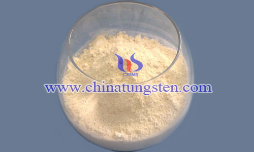
Rare earth market quotation in China: rare earth prices remain weak adjustment owing to weak demand side and cautious sentiment of traders. Most sellers reduce their offer levels for more deals.
China Molybdenum Prices - July 29, 2019
- Details
- Category: Tungsten's News
- Published on Monday, 29 July 2019 18:07
- Written by Shuxia
- Hits: 693
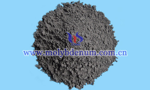
China molybdenum prices continue to rise in the week began on Monday July 29, 2019 on tight supply of molybdenum concentrate and active inquiry from downstream.
Molybdenum Disulphide Transistors Direct Tailoring After-Fabrication
- Details
- Category: Tungsten's News
- Published on Monday, 29 July 2019 17:47
- Written by rizhong
- Hits: 633
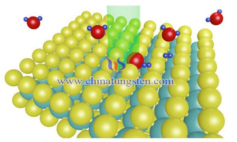
Making electronic devices from exfoliated 2-D materials can be tricky. The Daniel Granados team of IMDEA Nanociencia designed a solution that includes post-fabrication customization of MOS 2-FET transistors using pulsed focused electron beam-induced etching.
Transition metal disulfides are thin layers of 2-D atoms bound together by Van der Waals force. These materials exhibit thickness-dependent variations in their physical properties and can be used in different optoelectronic applications.
Atomic thin layers of MoS2 can be separated by micromechanical stripping, but manufacturing optoelectronic devices from mechanically stripped MoS2 is a complex process. Even with the deterministic stamping method, the geometry of the device is limited by the flake shape in all cases. Even when CVD (Chemical Vapor Deposition) technology is used, device fabrication is hindered by materials growing in the island, which have reduced size and different physical properties.
Therefore, it is very interesting to develop the technology of customizing device geometry after the manufacturing step is completed. The group of Prof. Daniel Granados at IMDEA Nanociencia proposed an intelligent solution by modifying the geometry of several field-effect transistors (FET) made of exfoliated MoS2. The proposed method uses focused electron beam induced etching (FEBIE) and pulsed electron beam variation. The beam uses a pattern generator to scan the surface into a designed geometry, modify the conduction channel between the source and drain of the transistor, and allow customized device performance.

Compared with the method using multiple manufacturing steps, this method has several advantages. First, it combines patterning and etching in one step rather than two-step nanofabrication. Secondly, it allows electronic and optical characterization before and after customization steps in a simple scheme. Lastly, pulsed FEBIE is a chemical method whose electron beam energy is lower than that of other studies (2.5 kV), which can reduce sample damage and prevent the distortion of MoS2 lattice. Because of these advantages, Granados et al. proposed nanoscissors. It is a significant alternative to expensive and time-consuming nanofabrication technologies, and has great potential for customization of post-fabrication with electrical and geometric characteristics of electronic and photoelectric devices.Making electronic devices from exfoliated 2-D materials can be tricky. The Daniel Granados team of IMDEA Nanociencia designed a solution that includes post-fabrication customization of MOS 2-FET transistors using pulsed focused electron beam-induced etching.
Transition metal disulfides are thin layers of 2-D atoms bound together by Van der Waals force. These materials exhibit thickness-dependent variations in their physical properties and can be used in different optoelectronic applications.
Atomic thin layers of MoS2 can be separated by micromechanical stripping, but manufacturing optoelectronic devices from mechanically stripped MoS2 is a complex process. Even with the deterministic stamping method, the geometry of the device is limited by the flake shape in all cases. Even when CVD (Chemical Vapor Deposition) technology is used, device fabrication is hindered by materials growing in the island, which have reduced size and different physical properties.
Therefore, it is very interesting to develop the technology of customizing device geometry after the manufacturing step is completed. The group of Prof. Daniel Granados at IMDEA Nanociencia proposed an intelligent solution by modifying the geometry of several field-effect transistors (FET) made of exfoliated MoS2. The proposed method uses focused electron beam induced etching (FEBIE) and pulsed electron beam variation. The beam uses a pattern generator to scan the surface into a designed geometry, modify the conduction channel between the source and drain of the transistor, and allow customized device performance.Compared with the method using multiple manufacturing steps, this method has several advantages. First, it combines patterning and etching in one step rather than two-step nanofabrication. Secondly, it allows electronic and optical characterization before and after customization steps in a simple scheme. Lastly, pulsed FEBIE is a chemical method whose electron beam energy is lower than that of other studies (2.5 kV), which can reduce sample damage and prevent the distortion of MoS2 lattice. Because of these advantages, Granados et al. proposed nanoscissors. It is a significant alternative to expensive and time-consuming nanofabrication technologies, and has great potential for customization of post-fabrication with electrical and geometric characteristics of electronic and photoelectric devices.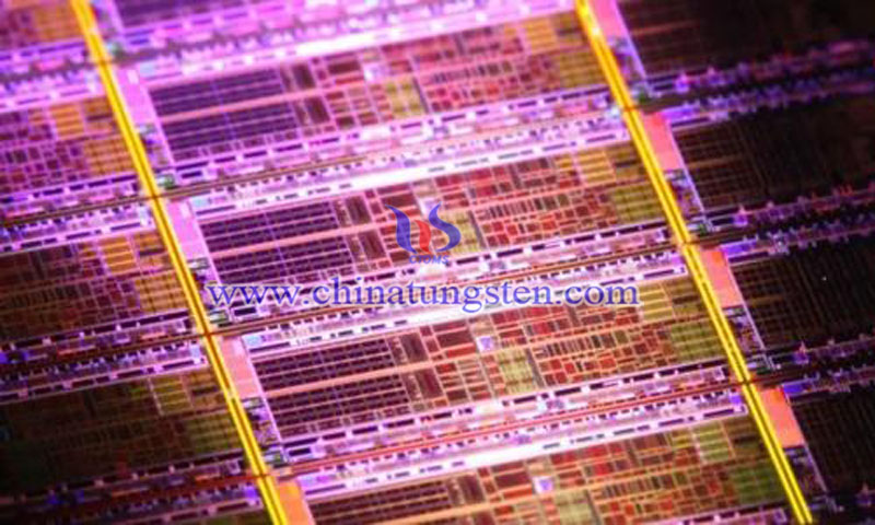
| Molybdenum Supplier: Chinatungsten Online www.molybdenum.com.cn | Tel.: 86 592 5129696; Fax: 86 592 5129797;Email:sales@chinatungsten.com |
| Tungsten News & Prices, 3G Version: http://3g.chinatungsten.com | Molybdenum News & Molybdenum Price: http://news.molybdenum.com.cn |
Physicists Study Light Propagation in 2D Molybdenum Diselenide
- Details
- Category: Tungsten's News
- Published on Monday, 29 July 2019 17:59
- Written by rizhong
- Hits: 652
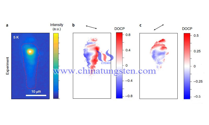
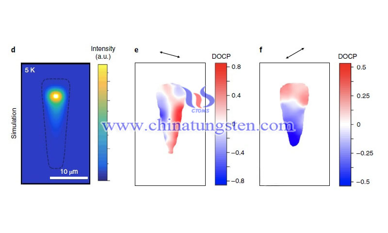
An international research team has studied how light propagation in the plane of the thinnest semiconductor crystal in the world. It is found that the spatial distribution of light polarization is similar to that of three-color rapana.
The research results open the door for the development of monatomic optical transistors - quantum computer components can be calculated at the speed of light. The study was published in Nature Nanotechnology. At present, photons are considered to be most suitable for transmitting information in quantum computers. These computers are still hypothetical, based on the laws of the quantum field, and can solve some problems more effectively than the most powerful supercomputers.
"I expect that in the near future, two-dimensional monatomic crystals will be used to transmit information in quantum devices," said Professor Alexey Kavokin, director of the Spin Optics Laboratory at St. Petersburg University.
Classical computers and supercomputers take a long time to complete, and quantum computing devices will be completed soon. That's the great danger of quantum technology - as dangerous as the atomic bomb. For example, with their help, bank protection systems can be cracked very quickly. That's why intensive work is under way today, including the creation of a means to protect quantum devices: quantum cryptography. Our work contributes to semiconductor quantum technology.

At present, it is impossible to achieve this state at temperatures above - 70 C. However, once suitable materials are found, the invention will enable power to be transmitted to any point on the earth without any loss, and develop a new generation of motors.
In March 2018, Alexey Kavokin's team predicted that the structure of superconducting metals such as aluminium could help overcome this challenge. At present, researchers at the University of St. Petersburg are trying to find ways to obtain theoretical and experimental evidence.
| Molybdenum Supplier: Chinatungsten Online www.molybdenum.com.cn | Tel.: 86 592 5129696; Fax: 86 592 5129797;Email:sales@chinatungsten.com |
| Tungsten News & Prices, 3G Version: http://3g.chinatungsten.com | Molybdenum News & Molybdenum Price: http://news.molybdenum.com.cn |
Electrochromic Tungsten Oxide Smart Glass Research or Boosting Fuel Cells Evolution
- Details
- Category: Tungsten's News
- Published on Monday, 29 July 2019 09:54
- Written by Caodan
- Hits: 764

Recent research has found that electrochromic tungsten oxide smart glass plate research or providing new ideas for fuel cells research and development. Smart glass is an energy-efficiency product found in newer windows of cars, buildings, and airplanes, slowly changes between transparent and tinted at the flip of a switch.
Read more: Electrochromic Tungsten Oxide Smart Glass Research or Boosting Fuel Cells Evolution



 sales@chinatungsten.com