What Are the Applications of Ammonium Metatungstate?
- Details
- Category: Tungsten Information
- Published on Thursday, 10 April 2025 17:40
- Written by Xiaoting
- Hits: 178
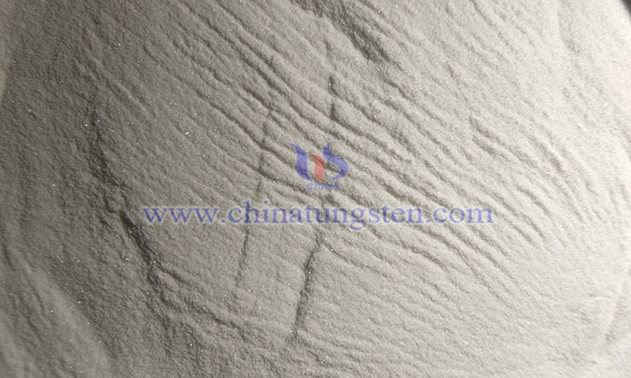
Ammonium metatungstate (AMT) produced by CTIA GROUP LTD is a high-purity white powder renowned for its excellent mechanical, chemical, and thermal properties. It finds widespread application in the preparation of metallic tungsten powder, catalyst production, the fireproofing industry, and the ceramics industry.
Read more: What Are the Applications of Ammonium Metatungstate?
Application of Ammonium Metatungstate in Ceramics
- Details
- Category: Tungsten Information
- Published on Thursday, 10 April 2025 17:40
- Written by Xiaoting
- Hits: 157
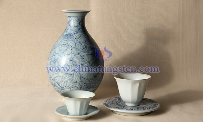
The application of ammonium metatungstate (AMT), a chemical compound of the transition metal tungsten produced by CTIA GROUP LTD, spans multiple fields. This is because AMT has unique chemical properties and thermal stability. Beyond serving as a crucial precursor for preparing tungsten-based materials, AMT is also a key additive in ceramics. Its roles in ceramics are primarily reflected in the following aspects:
Read more: Application of Ammonium Metatungstate in Ceramics
What Is Ammonium Metatungstate?
- Details
- Category: Tungsten Information
- Published on Thursday, 10 April 2025 17:34
- Written by Xiaoting
- Hits: 147
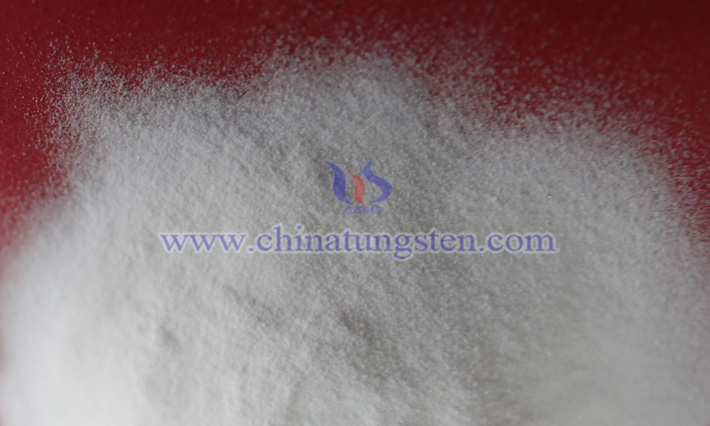
Ammonium metatungstate produced by CTIA GROUP LTD is an inorganic compound formed by the combination of ammonium ions (NH₄⁺) and complex polytungstate anions [H₂W₁₂O₄₀]⁶⁻. It is a white powder with the English name Ammonium Metatungstate (AMT), chemical formula H₂₈N₆O₄₁W₁₂, and CAS number 12333-11-8.
Production Method of Ammonium Metatungstate
- Details
- Category: Tungsten Information
- Published on Thursday, 10 April 2025 17:40
- Written by Xiaoting
- Hits: 165
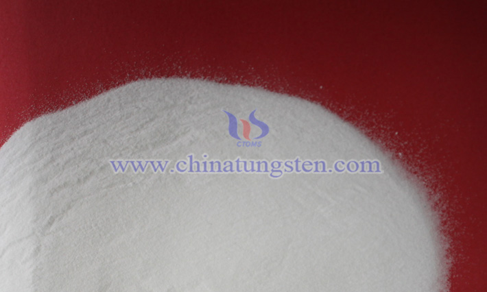
Ammonium metatungstate (AMT) is a white crystalline powder and an important tungsten chemical. It possesses good water solubility and high thermal stability, making it a key precursor in the preparation of metallic tungsten. Additionally, AMT is used in petrochemical industries to produce tungsten-based catalysts, enhances flame retardancy in fire-resistant fabrics, and improves various properties in the ceramics industry.
Performance of Cut-Resistant Tungsten Wire in High-Temperature Environments
- Details
- Category: Tungsten Information
- Published on Tuesday, 08 April 2025 19:41
- Written by Zhenghua
- Hits: 147
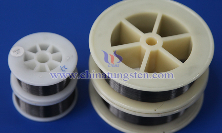
The performance of cut-resistant tungsten wire in high-temperature environments is significantly superior to many other metallic materials, primarily due to tungsten's inherent properties. Below is a detailed analysis of its high-temperature characteristics:
Read more: Performance of Cut-Resistant Tungsten Wire in High-Temperature Environments


 sales@chinatungsten.com