Tungsten-copper Thin Films Deposited by Ion Beam Sputtering
- 詳細
- カテゴリ: Tungsten Information
- 2019年7月28日(日曜)22:06に公開
- 参照数: 3503
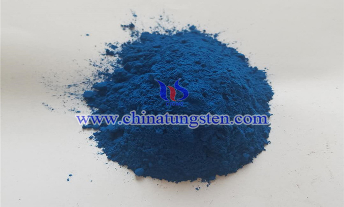
Tungsten-copper composite is one of the heat sink materials widely used in power devices. It has good thermal conductivity and thermal expansion coefficient close to that of Si, GaAs and other semiconductor cores. Density of composites is the main factor affecting the electrical conductivity, thermal conductivity and expansion properties of composites, and it is also the key technical index.

Powder metallurgy is the main method of traditional preparation of Cu-W composites. However, tungsten-copper thin films are required for electronic packaging. Magnetron sputtering deposition, ion beam sputtering deposition, ion beam irradiation and electron beam co-evaporation deposition are the main new methods for preparing tungsten-copper films. Some researchers have prepared tungsten-copper thin films by ion beam sputtering. The process includes:
The two sputtering targets have a water cooling device that can be adjusted up and down, and the target power is automatically controlled by the target current. The target material W has a purity of 99.9% and a size of Φ76*4. The distance from the substrate is 87cm and the angle is 30 degrees. The target Cu has a purity of 99.9% and a size of Φ76*4. The distance from the substrate is 100cm and the vertical is 30 degrees. The distance between the two targets is 23cm. . The substrate used was a sheet of Φ 25 mm and a thickness of 4 mm. The substrate was first washed with acetone for 10 minutes and then washed with alcohol for 10 minutes. After being dried in a heating oven, the ion beam was bombarded for 30 minutes with high energy bombardment. A water cooling system was installed under the sample stage and rotated at 15 rpm. The working gas is argon gas with a purity of 99.9%. The gas pressure is controlled by a vacuum gauge. The gas flow rate is controlled by a flow meter. The Ar+ energy of the tungsten sputtering target is adjusted to 3.6 keV, the beam current is 60 mA, and the copper sputtering target Ar+ energy is adjusted to 1.9 keV. The flow rate is 25 mA; the energy of the low energy auxiliary deposition source is adjusted to 0.3 keV, the beam current is 21 mA, and after sputtering for 1 hour, a high thermal conductivity low expansion copper-tungsten composite film is obtained.
The fabricated amorphous copper-tungsten composite films with high thermal conductivity and low expansion, i.e. pseudoalloys, not only have good thermal conductivity and similar thermal expansion coefficients to SiGaAs and other semiconductors, but also have sufficient bonding strength, good processability, light weight and low cost, which can be applied to ultrafine semiconductor devices.


 sales@chinatungsten.com