A Chinese Company Mastered the Manufacture of Tungsten Targets
- Details
- Category: Tungsten's News
- Published on Tuesday, 17 July 2018 15:41
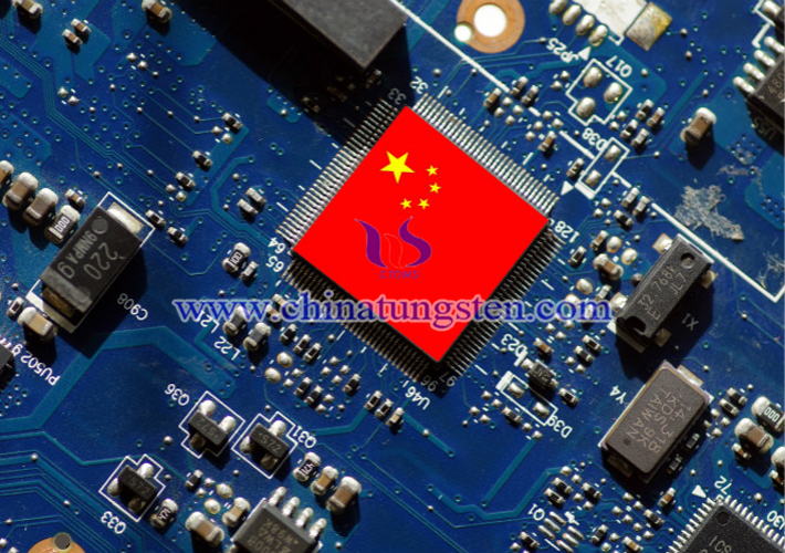
Semiconductor large-scale integrated circuits (chips) are the world's most advanced manufacturing technology. For a long time, China has been lagging behind developed countries in this field. The world's most advanced chip technology has been monopolized by western countries. China's annual chip import costs have surpassed crude oil, and it has to withstand the risk of Americans' restrictions and prohibitions from time to time.
It is well known that China is the world’s largest producer of mobile phones and computers. Although 25 percent of the world’s mobile phones are made by China. China is highly dependent on foreign tech in its semiconductor industry, importing 90 percent of its chips in order to power the fast-growing electronic industry. The inner problem is that China hasn’t master the advanced technology of manufacturing the chips. What’s more, the recent ZTE event has remind Chinese that the importance of breaking through the monopoly on the chips from the United States.
Thin film science is a very important area in the development and manufacture of semiconductor devices. A thin transparent conductive film coated on the functional layer of a semiconductor chip with precision equipment. This layer is less than one-fifth of the diameter of a hair to achieve the physicochemical properties of the semiconductor metal. They are what called thin films. In the metallization process of chip manufacturing, tungsten oxide thin film is a widely studied functional material, mainly used as an integrated circuit diffusion barrier layer, a bonding layer, and a large integrated circuit memory electrode.

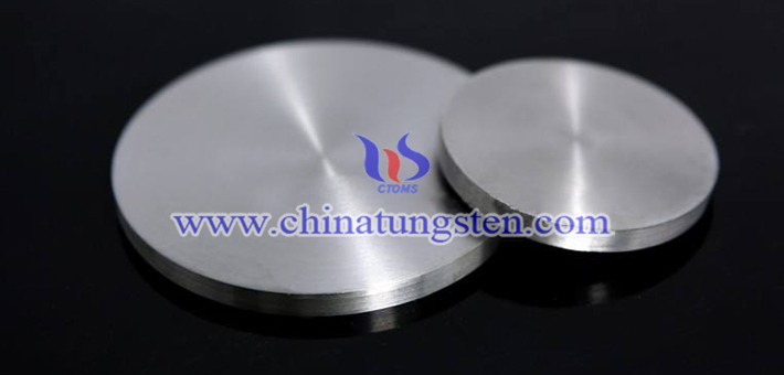
The key to a plated film is what is called a "target." The performance of the target directly affects the performance of the film, which affects the performance and benefits of the chip manufacturing. Sputtering is one of the main techniques for preparing thin film materials. It bombards the target by high-speed moving ions, and the generated atoms are emitted to accumulate on the surface of the substrate to form a coating. The bombarded solid is the raw material for depositing the thin film by sputtering. This raw material is called a sputtering target. This is an important matrix for the tungsten oxide film to achieve its functional transition in semiconductor devices.
Due to its high melting point, tungsten targets are mainly prepared by powder metallurgy methods. For tungsten targets used in chip manufacturing, only the United States, Japan and other countries have mastered the relevant manufacturing technologies. However, last year, the CCTV’s documentary "Amazing China" filmed a company in Ningbo, China achieved breakthroughs in tungsten targets. It ended the history that metal targets must rely on imports, and even make China reaching a leading position in the field of tungsten targets.

It has a strict requirement for the purity of tungsten targets in the semiconductor integrated circuits. Generally, the purity of targets is required to be above 99.999%. At the same time, the compactness of the target has an important influence on the coating process and the performance of the film. The density of the target does not only affect the deposition rate during sputtering, the density of the sputtered film particles and the discharge phenomenon, but also affects the electrical and chemical properties of the film. In short, the denser the target, the lower the density of the sputtered film particles, the weaker the discharge phenomenon, and the better the performance of the film.
It is told that the leader of this Chinese company is a returnee entrepreneur. For high-purity tungsten targets, the manufacturing technology required is the most advanced in the world. However, this Chinese team broke through the technical difficulties in the manufacturing of high-purity tungsten, completely broke the western monopoly, and no longer has to rely on exports.
- Tungsten Manufacturer & Supplier, Chinatungsten Online: www.chinatungsten.com
- Tungsten News & Prices of China Tungsten Industry Association: www.ctia.com.cn
- Molybdenum News & Price: news.molybdenum.com.cn
- Tel.: 86 592 5129696; Fax: 86 592 5129797; Email: sales@chinatungsten.com


 sales@chinatungsten.com