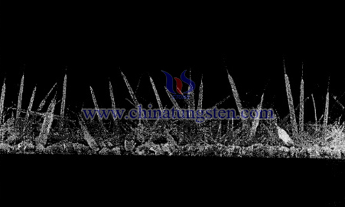
Tungsten Oxide Pencil-like Nanostructure Arrays
- Details
- Category: Tungsten Information
- Published on Saturday, 20 April 2019 17:19
Tungsten oxide is an important semiconductor material. It is widely used in electrochromic devices, gas chromic devices, photovoltaic cells and other photovoltaic devices.

For example, a pencil-like tungsten oxide nanostructure array, which can be used to improve the field enhancement factor of the emitter and reduce the shielding effect of field emission, is a field emission material to achieve low field emission. Some scholars have studied this material and prepared it by the following methods:
1.Monocrystalline silicon wafers were used as substrates and cleaned by ultrasonic cleaning with acetone and absolute ethanol.
2.Place the silicon wafer substrate in the thermal evaporation device, clean the substrate, place it in the vacuum evaporation chamber, and keep a certain distance from the evaporation source.
(1)Inert gas is introduced as the ambient atmosphere, and trace oxygen (e.g. 3sccm) is introduced to heat the evaporation source and substrate at the evaporation chamber pressure of about 20Pa; within about 30 minutes, the evaporation source temperature (Tb) is heated from room temperature to Tb1 (the optimum value is 1150 ℃), and the substrate temperature (Ts) is heated to Ts1 (the optimum value is 750 ℃), so that tungsten oxide nucleates on the substrate; finally, Tb and Ts fractions are heated. The nanorod arrays were formed by maintaining T2 (range 10 minutes) near Tb2 (Tb2 = Tb1) and Ts2 (Ts2 = Ts1).
(2)Rapidly increase Tb and Ts to Tb3 (range: 1250-1400 C, optimum value is 1300 ℃) and Ts3 (optimum value is 850 ℃), maintain T3 (range is 10 minutes), use evaporation and sintering effect to reduce the density of nanorods, that is, in this process, some of the nanorods generated in step (4) are evaporated, while others are connected with several nearby nanorods. The densities of nanorods are reduced by forming large diameter nanorods together.
(3)Rapidly reduce Tb and Ts to Tb4 (the optimum value is 1100 ℃) and Ts4 (the optimum value is 700 C), respectively, and maintain for 10 minutes to form small diameter nanorods on the top of large diameter nanorods.
(4)Rapidly reduce Tb and Ts to Tb5 (the optimum value is 950 ℃) and Ts5 (50 ~150 ℃ smaller than Ts4, the optimum value is 600 ℃, maintain T5 (the optimum value is 10 minutes), and form nano-tip on the nanorod with small diameter;
(5)Cool Tb and Ts to room temperature and take out samples. The tungsten oxide nanoparticles, nanorod arrays, low density nanorod arrays and pencil-like nanostructure arrays were grown on the substrate in turn.
Compared with the field emission properties of some reported tungsten oxide nanomaterials, the W8O49 pencil-like nanostructure arrays have been fabricated by multi-step heating method. The arrays have excellent field emission properties and can be used as cold cathode materials in cold cathode electronic sources, field emission flat panel displays and cold cathode light emitting devices.
- Tungsten Oxide Manufacturer & Supplier, Chinatungsten Online: www.tungsten-oxide.com
- Tungsten News & Prices of China Tungsten Industry Association: www.ctia.com.cn
- Molybdenum News & Price: news.molybdenum.com.cn
- Tel.: 86 592 5129696; Fax: 86 592 5129797; Email: sales@chinatungsten.com


 sales@chinatungsten.com