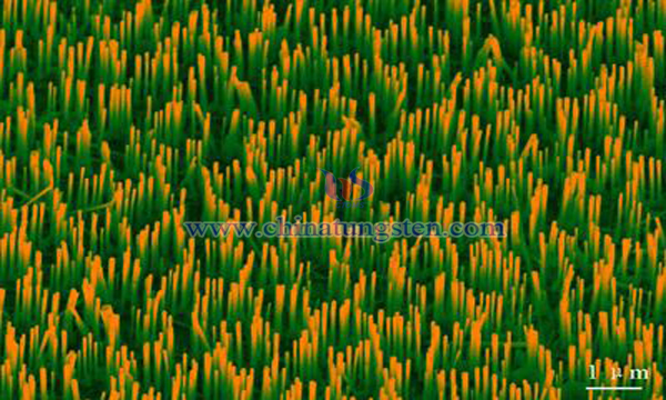
Five Common Schemes for Tungsten Nanowires Preparation
- Details
- Category: Tungsten Information
- Published on Wednesday, 22 May 2019 16:26
Tungsten metal has excellent physical and chemical properties, such as high melting point (3410 ℃), high density (19.35g/cm3), high conductivity/thermal conductivity, excellent high temperature strength and hardness, low work escape, very low thermal expansion coefficient and vapor pressure, and good corrosion resistance, which makes tungsten an important functional material and high temperature structural material.

The main problems of tungsten are intrinsic brittleness, recrystallization embrittlement and irradiation catalysis of body-centered cubic. The brittleness limits the processing and serviceability of tungsten greatly. For example, in the development of ITER, the most important task of researchers is to solve the brittleness of tungsten.
At present, there are five schemes for preparing tungsten nanowires abroad.
Firstly, tungsten nanowires were synthesized by vapor deposition combined with low melting point metal catalysts. The main principle is that W nanowhiskers were successfully synthesized by vapor deposition at 850 ℃ and under VSS growth mechanism using Ni, Fe-Ni and Co-Ni as catalysts. However, the metal catalysts used in this method will pollute the synthesized products and affect the performance of the products. It is difficult to prepare one-dimensional nanostructures of monomers, and the mechanism of this method limits the large-scale preparation of tungsten wires.
Secondly, tungsten nanowires are prepared by plasma RF etching of very fine tungsten wires. The tungsten nanowires with 25 micron diameter are etched to 40 nanometers by using Ar + plasma as sputtering ion. However, this method is only suitable for the preparation of single one-dimensional W nanowires, and is not suitable for the controllable preparation of large-scale one-dimensional W nanowire arrays.
Thirdly, tungsten nanowires are prepared by electron beam induced deposition. This method uses high-energy electrons emitted by sub-nanometer probes to induce the growth of one-dimensional W nanowires from the tip. After ionizing the front-end precursor molecules, the W nanowires with several nanometers in diameter are self-assembled by reverse deposition at the top. However, this method, like etching method, is only suitable for single one-dimensional W nanowires. The preparation can not be produced in large quantities.
Fourthly, single-crystal tungsten nanowires were prepared by deposition of gas molecules of organic metal compounds or precursors under the action of electron beam in thermal or cold field emitters. For example, single-crystal W nanowires with diameters of 20-80 nm and lengths of up to 30 um were successfully prepared by sodium tungstate and hexadecyltrimethylammonium bromide. However, one-dimensional W nanowires prepared by this method usually have more than one-dimensional W nanowires. Crystal structure affects its performance, and impurities such as precursors will affect the purity of the prepared tungsten wire.
Fifthly, tungsten nanowires are prepared by self-assembly using surfactants. This method is a process in which atoms, molecules or molecular groups of tungsten nanowires are arranged automatically from bottom to top to form ordered structures without external factors. Some scholars have prepared W nanowires arrays with flat rod-like structures of 10-50 nm in diameter by self-assembly of tungsten films. This method can be used without introducing foreign catalysts. One-dimensional W nano-material arrays with high purity and good crystallization were fabricated. The cost of synthesis process was low and the operation was simple. However, the length and diameter of the products were not uniformly controlled, and the single batch yield was low.
- Tungsten Manufacturer & Supplier, Chinatungsten Online: www.chinatungsten.com
- Tungsten News & Prices of China Tungsten Industry Association: www.ctia.com.cn
- Molybdenum News & Price: news.molybdenum.com.cn
- Tel.: 86 592 5129696; Fax: 86 592 5129797; Email: sales@chinatungsten.com


 sales@chinatungsten.com