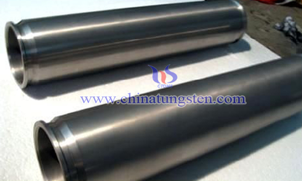
Exploration on Preparation Process of Large Size Tungsten Target
- Details
- Category: Tungsten Information
- Published on Saturday, 09 February 2019 23:23
Sputtering is one of the main technologies for preparing thin film materials. Atomics emitted by high-speed moving ions bombarding the target accumulate on the surface of the substrate to form a coating. The bombarded solid is the raw material for deposition of thin film by sputtering, which is called sputtering target.

Thin films deposited by target sputtering need to have the advantages of high density and good adhesion. Rare metal tungsten has been widely used in semiconductor integrated circuits, solar photovoltaic and other sputtering fields due to its high melting point, high strength, low thermal expansion coefficient, low resistivity and good thermal stability.
Tungsten target is mainly used as diffusion barrier layer of integrated circuit and memory electrode of large integrated circuit in semiconductor field. Semiconductor integrated circuits have high requirements for the purity of target materials. Generally, the purity of target materials is required to be more than 99.999%. At the same time, the compactness of the target material also has an important influence on the coating process and the performance of the film. The compactness of the target material not only affects the deposition rate, the density of the sputtered film particles and the discharge phenomenon, but also affects the electrical and optical properties of the sputtered film. The denser the target, the lower the density of the sputtered film particles, the weaker the discharge phenomenon, and the better the performance of the film.
Because of its high melting point, tungsten target is mainly prepared by powder metallurgy. At present, tungsten targets for semiconductor are usually sintered directly into final products by hot pressing or hot isostatic pressing without subsequent pressure processing. The density of tungsten targets can reach about 99% of the theoretical density. With the rapid development of semiconductor technology, the degree of integration is getting higher and higher. The number of integrated devices per unit area of monocrystalline silicon wafer increases exponentially. The mainstream size of silicon wafer has gradually developed from 12 inches (300 mm) to 18 inches (450 mm), so the size requirement of sputtering target is also increasing. To produce larger tungsten target by hot isostatic pressing requires high equipment input, and the density of the product is difficult to achieve full density. Therefore, how to prepare large tungsten target has become the focus of tungsten products manufacturing field.
The sintered tungsten slab with a density of 18.3g/cm3 was prepared by using suitable raw materials, reasonable process and parameters. The large-size high-purity tungsten target with a purity of 99.999%, a density of 99.5% and a grain size of less than 100 um was prepared by hot rolling, annealing and machining.
- Tungsten Manufacturer & Supplier, Chinatungsten Online: www.chinatungsten.com
- Tungsten News & Prices of China Tungsten Industry Association: www.ctia.com.cn
- Molybdenum News & Price: news.molybdenum.com.cn
- Tel.: 86 592 5129696; Fax: 86 592 5129797; Email: sales@chinatungsten.com


 sales@chinatungsten.com