Tungsten Oxide Ceramic Barrier Model
- Details
- Category: Tungsten Information
- Published on Tuesday, 13 March 2018 08:46
The barrier model is a barrier formed within the semiconductor when the metal and the semiconductor are in contact. For metals and semiconductors, they have different work functions. The barrier model was originally thought to be caused by the fact that metals and semiconductors have different work functions and the contact potential differences they generate when they are in contact. Experiments in recent years have shown that semiconductor surface states have a very important influence on the formation of barriers.
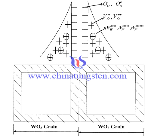
The picture shows the barrier model of tungsten oxide ceramics. From the figure, the oxygen vacancies in the tungsten oxide ceramics can provide electrons to the semiconductors on the one hand, and have fewer defects as donor levels, making the resistance of the crystal grains smaller. On the other hand, sites for oxygen ions adsorbed on the grain boundary are provided. Based on the grain size, we mentioned earlier that this is related to the concentration of oxygen vacancies formed by the grains. Because the grain size of the sample sintered at 900-1000°C is small, indicating a small material transmission rate, the concentration of oxygen vacancies that determine the material transfer rate is small.

Therefore, the grain boundary barrier formed by oxygen adsorption at the grain boundary has a low height, the grain resistance is large, and the grain boundary grain resistance difference is small. When the voltage is applied, the lower barrier of the grain boundary makes the current density larger; when the voltage increases to a certain degree, the grain resistance starts to function, resulting in nonlinear electrical characteristics. According to the barrier model, the degree of grain boundary oxidation of samples sintered above 1100°C should be higher. The pressure sensitive properties should be better than those sintered at 1100°C. However, we see that samples sintered at 1150°C have the same non-linear electrical properties in the current density range of 10-100mA as the samples sintered at 900-1100°C.

The resistance of the sample sintered at 1150°C is minimal compared to other samples. This is caused by the combined effects of two reasons. On the one hand, due to the larger concentration of oxygen vacancies produced by the tungsten oxide ceramic grains at a temperature of 1150°C, the oxygen adsorbed at the grain boundary during the cooling process is used to fill up the oxygen crystal lattice vacancies in the grain boundary. When the excess adsorbed oxygen ions begin to form barriers at the grain boundaries, the temperature in the sintering furnace has decreased much. The oxygen adsorption efficiency is low, resulting in a lower barrier to the formation of oxygen ions at the grain boundary. On the other hand, the grain size of the tungsten oxide ceramics sintered at 1150°C is the largest, resulting in the smallest varistor voltage.
- Tungsten Oxide Manufacturer & Supplier, Chinatungsten Online: www.tungsten-oxide.com
- Tungsten News & Prices of China Tungsten Industry Association: www.ctia.com.cn
- Molybdenum News & Price: news.molybdenum.com.cn
- Tel.: 86 592 5129696; Fax: 86 592 5129797; Email: sales@chinatungsten.com


 sales@chinatungsten.com